

Although a Printed Circuit Board (PCB) is a common term in the electrical and electronics arena, few are aware of its origins, requirements, and design requirements. Before PCBs evolved to their present state, components had to be interconnected by wiring from one point to another. Not only was this laborious, but also susceptible to frequent failures at junctions and places where wire insulation aged and cracked and formed short circuits.
This led people to move on to wire wrapping. They wrapped a small gauge wire around a metal post at individual connection points. This created a connection, which was highly durable, gas-tight, and easily changeable.
However, with electronics moving towards integrated circuits, and SMDs, the number and complexity of electronic components in gadgets increased to a great extent, while consumers wanted reductions in the size and cost of electronic products. To meet these demands, designers and manufacturers developed the printed circuit board or PCB.
Functions of a PCB
A PCB replaces the point-to-point wire connections with copper traces printed on to a non-conducting board or substrate, hence the name. The PCB also has space for mounting the other required electronic components onboard, and this makes the soldered PCB a major subassembly within an electronic device today. Apart from mechanically anchoring the components to the PCB, solder also forms a good electrical connection between the component leads and copper traces on the PCB.
Types of PCBs
Single-sided PCBs have the copper traces only on one side of the non-conducting substrate. To accommodate circuits of higher complexity on smaller boards, the single-sided PCB soon gave way to double-sided ones, where the copper traces were present on both sides of the substrate. As circuit complexity increased further, designers went on to design PCBs n multiple layers, with vias to interconnect the copper traces on each layer. The complexity of modern computer boards today requires them to accommodate as many as 16+ layers.
Parts of a PCB
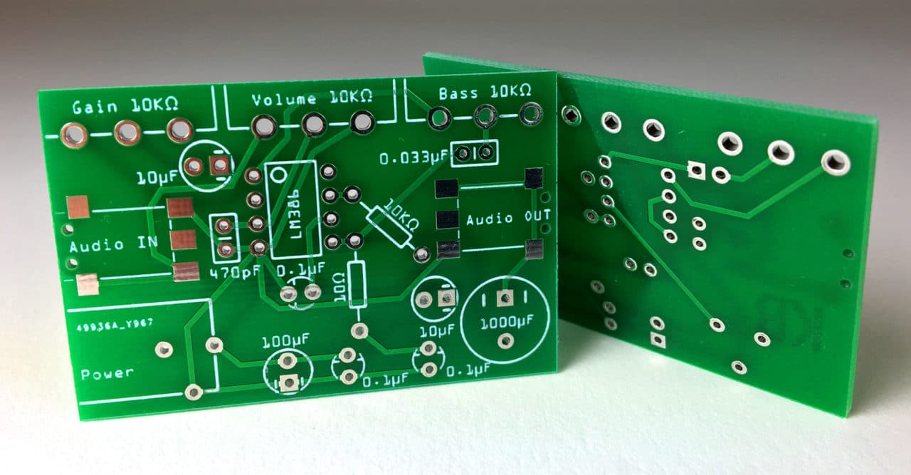
The non-conductive substrate of a typical PCB is made of paper phenolic or glass epoxy, and is a rigid structure. Special PCBs may be made of other material such as Polyimide or Kapton, and may be flexible rather than rigid. Apart from the non-conductive substrate and copper traces, a green insulating mask, also known as soldermask, protects the PCB, leaving out only parts of traces or pads that will undergo soldering. Flexible boards use coverlays in place of the green soldermask.
To aid assembly and to allow indicators for a better understanding of the PCB, designers often apply a light colored slikscreen layer on top of the soldermask layer, thereby adding letters, numbers, and symbols to the PCB. For instance, silkscreen labels may indicate the function of each pin of a connector or the polarity of an LED.
Advantages of using PCBs
A PCB offers a solid surface on which to mount components that make up an electronic equipment, in an organized and orderly manner. The PCB also provides the required insulation between components to allow them to function properly and dissipate heat. In short, a PCB is one of the factors allowing designers to make smaller and more compact electronic equipment.
Designing a Printed Circuit Board
To design a PCB, one must understand the process of its fabrication. The substrate initially has a layer of copper on one or both its side—depending on whether it is finally to be a single-sided PCB or a double-sided one. The designer decides the pattern of copper traces that will eventually remain on the PCB, and the fabricator transfers the pattern on to the copper layer by a process known as photolithography. The fabricator then removes the excess copper by chemical etching. After drilling necessary holes for vias and for accommodating leads of through-hole components, the fabricator covers the copper traces with soldermask and silkscreen.
Deciding the Physical Size
The most common method of designing a PCB starts by estimating the amount of space necessary to hold all the components within the equipment. If the available space is inadequate, the designer has to either use smaller sized components or increase the space within the equipment—a compromise often provides the solution. This exercise also defines the physical boundaries of the PCB, and its method of mounting within the equipment.
Placement of Components
A PCB designer then places the electronic components or rather, their footprints, within the PCB boundary, and arranges them for maximum ease of connectivity. For instance, a connector that will interconnect the PCB to a panel on top of the equipment would optimally be placed on the outer edge of the PCB and nearer to the panel. Similarly, the designer is likely to place components associated with an IC closer to it to reduce the complexity of connections.
Manual Design
Earlier, designers would arrange the component footprints using self-adhesive tapes and pads on to a Mylar sheet in a 4:1 ratio. On completion, an industrial camera would produce a photographic film of the design correct to actual proportions, and the fabricator used the film to transfer the pattern on to the copper layer. The advent of computers and easily available PCB design software packages has made the above process obsolete.
Computer Aided Design
Today, designers rely on CAD or computer aided PCB design software packages to produce the copper trace pattern for the fabricator. The CAD package usually has a database containing the symbols, footprints, and other details of the numerous electronic components that designers use. CAD packages for PCB design work in three parts—schematic capture for drawing the circuit schematic, an autorouter for creating the interconnections, and a printer part for generating the necessary output files.
The database in the CAD package provides the designer with symbols for the various components, while the designer has to define the specific footprint for each component they use. As the designer interconnects the pins of different components, the software package keeps track by generating a net list.
The autorouter uses the net list to place the defined footprints within the boundary and allows the designer to arrange them most optimally. On satisfactory completion, the autorouter proceeds to interconnect the components with traces of default width. The designer can define the width of specific trace to be greater than or less than the default width and the autorouter will try to reroute to accommodate the change. If the design is impossible to complete within a single side, the autorouter will suggest the designer use two or more layers. The PCB industry uses Gerber files as the standard mode of transferring engineering information to the fabricator for manufacturing the PCB.