WHY SHOULD YOU GET YOUR PCB BOARD DESIGN DONE BY RIOSH?
- RioSH is a firm believer in getting it right the first time. RioSH has exhaustive techniques to ensure all the entrapped errors are corrected before the product is brought to you. Thus saving your time, cost, and a frustratingly vicious cycle of incorrect outputs and alterations to rectify it.
- RioSH specializes in electronic product design including PCB design services. They also provide prototyping services so that you can test your device’s compatibility with the PCB before bulk manufacturing.
- RioSH has 16+ years of excellent experience in the contract designing and manufacturing of a vast variety of electronic products which is cost-effective while not compromising the quality.
Based in Bangalore, India having an immense talent pool with low operating costs, RioSH aims to provide our customers who want to outsource their design, programming & manufacturing at lower costs & improve quality levels.
PCB DESIGNING METHOD
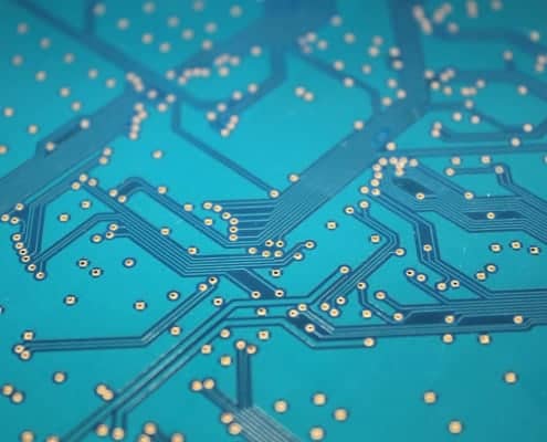
PCB is an acronym for Printed Circuit Board. PCB electrically connects the electronic components through conductive tracks and pads. These components are soldered onto the PCB to provide electrical connectivity and to fasten them onto the board. It is the base of the majority of electrical circuits providing it mechanical support and electronic connectivity to the electronic components and other integrated circuits. A simple PCB can be designed by laminating a slight layer of conducting material on top of an insulating substrate. The electronic components are then mounted on the circuit board and soldered into place which in turn saves a lot of effort debugging the circuitry for faults.
The PCB consists of alternating layers of different materials laminated with adhesive and heat resulting in a single object. The layers include:
- Silkscreen: this top layer adds the numbers, letters, and symbols to the PCB that allow for easy assembly and a better understanding of the board. The labels on the silkscreen indicate the function of each pin on the LED on the board.
- Soldermask: this layer gives the PCB its distinctive green color
- Copper: this layer is laminated to the PCB through adhesive and heat. The thickness of the copper is determined by the weight, in ounces per square foot.
- The substrate (FR4): this is the base material and is usually fiberglass. This layer gives the PBB thickness and rigidity. Aluminum is also used instead of fiberglass. Aluminum is preferred because it is low cost, environmentally friendly and durable.
Depending upon the PCB design there are multiple types of PCB including:
Single Sided PCB
A single sided PCB design consists of a single layer of the substrate followed by a thin metal coat on one side. Conventionally, after the base metal plating, a protective solder mask is applied along with the silkscreen mask to mark out the parts of the board. The Double sided PCB design services include solid state drives, printers, calculators, cameras, radio and stereo equipment, and power supplies.
Double Sided PCB
This PCB design is different and more useful than the single-sided PCB because it has metal conductive layers on both sides of the substrate. The holes drilled in the PCB allows the connectivity between the circuits on either side of the board. The double-sided PCB design allows the circuits and electronic components to connect to the other side using two techniques: through hole or surface mount. Through holes allows the connections via small wires also known as leads, passed through the holes and soldered to the respective component. The surface mount technology uses the board as a wiring surface for components. This PCB design service allows you to make compact circuits and takes much lesser space as compared to other PCBs. The Double sided PCB design services include Automotive dashboards, Power supplies, HVAC systems, LED lighting, Amplifiers and Vending machines.
Multi-Layer PCB
Multi-Layer PCBs further enhance the intricacy of PCB design by having from three to as many as ten or twelve substrate layers. The layers encapsulated between the two outer planes are power plants which supply the circuit with power. The Multilayer PCB design reduces the electromagnetic interference created by the circuits, by placing signal levelers in the middle of the power planes. The Multi-Layer PCB services include heavy equipment like computers, GPS technology, File servers, Data storage, Satellite systems, Weather analysis, and Medical machinery.
Rigid PCB
The PCB designs can also vary in rigidities along with the number of layers. When thinking of a circuit board an inflexible printed circuit board comes to our mind and this PCB design is produced by using fiberglass as a substrate. This keeps it from twisting or bending and keeps the shape intact. They come in single, double or multilayer forms. The rigid PCB design service can include any device’s circuit boards which need to be in the same shape throughout its lifespan. For example the motherboard inside the computer.
Flexible PCB
The PCB design can be altered to make it flexible by using flexible materials like plastic but the fabrication costs tend to be greater than the rigid PCBs. They are very efficient in terms of cost and weight as one PCB covers the area in which multiple PCBS would be needed.
Rigid-Flex PCB
Rigid-Flex PCB design is the best possible merger of rigid and flexible PCBs having rigid PCBs attached to flexible PCBs.
PCB DESIGN
A PCB can also be designed according to your technological needs thus being the best possible fit to assemble your circuit. It starts with a PCB designer who gathers all the product specifications and the requirements for your circuitry. Then using the best strategic design techniques he creates a best-fit PCB design to cater your needs ensuring it meets the standards and competitors products in the market. Here are some steps you can follow to design a PCB:
PCB Design using software:
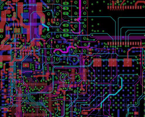
Drawing a schematic circuit diagram is the most crucial step of PCB design and should never be compromised or overlooked. For that, you need designing software such as Eagle, CAD, Allegro, ExpressPCB or Multisim software. A PCB design simulation contains a whole package that you need in order to build a circuit. Eagle provides a variety of libraries, easy Graphical User Interface, and the design can be altered according to requirements found in later stages or a project.
Schematic capture:
Make the schematic diagrams which can be entered into the schematic capture tool. After the completion and simulation of the desired circuit, the schematic capture cis contained within a file and is converted into a format which is called netlist. It contains all the tiny but crucial information such as circuit nodes, component pins and the respective pin connections with the modes or nets. Eagle performs algorithms on PCB designs in order to ensure no errors or faulty connections go undetected thus giving us the desired outputs. It is designed keeping the width, board edge spacing, trace, hole spacing and while sizes under consideration.
- Open the Eagle PCB design software.
- A window having a horizontal bar will appear.
- Open the dropdown menu and select a new design.
- Using the libraries in Eagle PCB design software pick symbols, components from the vertical bars.
- Make proper connections and add ratings of each element according to requirements.
- 1after you are done designing, open text editor varriages from the command toolbar in Eagle. Clicking on it opens a new window showing the film diagram or the layout of your circuit in black background.
From file to the film:
The next step involves printing the PCB of the schematic design producing the desired output. Manufactures performs DFM checks on the circuit and then finalize it to generate a film from a circuit board diagram of the PCB layout software. A highly precise laser jet printer is used by the plotters to provide incredibly detailed PCB design. A negative image is created from the Eagle PCB design on a plastic sheet which is then fabricated and assembled. As specified in the Eagle PCB design the circuit board is manufactured in which the inner layer black ink represents the conductive copper metal and the clear portion is the non-conducting material. The outer layers are the opposite. In the case of multiple films, the Eagle PCB design is done in a way that they are perfectly aligned before registration holes are punched.
Testing:
Once manufactured the PCB is tested to ensure proper structure. Every possible output is tested to ensure proper functionality. PCB testing is of two types:
- Black box testing: this testing only involves testing inputs and outputs without looking at any specifics.
- White Box testing: this testing is more detailed and involves testing every possible pathway to ensure there is no failure.